(I) Introduction of Nanoelectronics Center
1)Funding support
One Funding support is from Chongqing Distinguished Young Scientist Program 2013(0.6M RMB) and anotherfunding support is from Chongqing Important Research&Development Program 2013(3M RMB).
2)Lab&Equipments
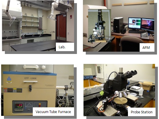
We have a commonlab with 160 m2where equipment for nanomaterials synthesis and property characterization locates, including 1200℃ high temperature CVD tube furnace for synthesizing ZnO nanowires/nanorods, hydrothermal method system for growing nanowires in low temperature,probe station system for characterizing electronic property of nanodevice,Atomic Force Microscopy(AFM) system for mechanical and electronical property characterization of nanostrucuted materials, and sample process systems, such asiron milling system, spinner,RF sputtering system, optical microscopy, 532nm and 633nm laser system, anti-vibration platform, optical spectrum system,fume
3) Research Team
A research team with ten members is proposed to be set up, including two professors,four associate professors,two assistant professors, and two research scientists. By now, three members, including one professor, one associate professor, and one research scientist,start to work for the center.More members are coming with the progress of ongoing recruiting process.
4)Important achievements
The research goal of Nanoelectronics Center to achieve distinguished research results for both scientific understanding and industrial application. Projects includenanosystem for green power source with function of harvesting energy and electricity storage dual function. Data storage system based on nanostrucutured materials, Photoelectric nanosensor system for accurately detecting and tracking tiny light spot, etc. All the ongoing projects are integrated to one goal: developing nanoelectrics by bottom-up method to replace microelectronics.
(II)Research Area
he key research projects for next few years of Nanoelectronics Center will focus on nanomaterials for energy harvesting and storage, nanodevice for data storage, Photodetecting system with ultra-high resolution using photoelectric nanowires,and nanomaterial enhanced polymer lithium ion battery technology.
(III) Research Group
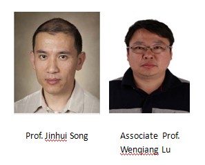
Nanoelectronics Center leader,professor Jinhui Song,who got his Ph.D from Georgia Institute of Technology(USA) in 2008, is awarded with Chongqing Distinguished Young Scientist in 2013.He joinedThe University of Alabama(Tuscaloosa) as assistant professor(Tenure Track) after he finished his post-doctor from Georgia Institute of Technology(USA). He received his full professor position from Chongqing Institute of Green and intelligent Technology since 2013. Prof. Song has published 47 papers on peer-reviewed professional journals, like Science,Nano Letters, Advanced Materials,Advanced Functional Materials,JACS,ACS Nano, Nano Research, Nanotechnology, J. Mater. Chem.APL,Phys.Chem.Chem.Phys. etc.By Sep. 2013, the total citation for his work has reached 5000 times with h-index of 28. Prof. Song also poessesses three USpatterns and authored5 scientific books. Currently, all members of Nanoelectronics Center have research and study experience oversea and with an average age of 31.
(IV)Achivements
1) Lab Construction
The Nanoelectronics Center has set up high temperature tube furnace for synthesizing nanomaterials by high temperature CVD method and hydrothermal system for synthesizing nanomaterials by low temperature wet chemical method.Besides, other experiment facilities, such as optoelectronic property characterization system and Atomic Force Microscopy(AFM) system for mechanic/electronic and nanowires surface characterization, and more are all set up.
2) Reserch Results
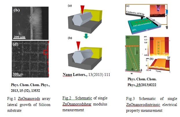
Recently, center has discovered a simple and effective vapor deposition method for directly growing ultra-long, laterally aligned, zincoxide (ZnO) nanorod arrays only on the side edges of a bare silicon (Si) substrate without using any catalystsand precursors. The growth on the top surface of the substrate is restrained by controlling the flow of sourcevapor in a tube furnace through the chemical vapor solid process. the lateral, ultra-long ZnO nanorods grown on orthogonalsilicon microelectrodes are achieved and could be expected to find important applications in a bottom-upway of fabricating the next generation nanoelectronics.The work was published on Phys. Chem. Chem. Phys..(2013, 15 (32), 13532-13537, IF 3.7)See fig.1.
Another discovery by the center is an innovative technique forthe direct measurement on the shear modulus of an individualnanorod. This measurement is based on atomic forcemicroscopy (AFM) and microfabrication techniques. Ananorod is first aligned along the edge of a small trench in asilicon substrate, and then one end of the nanorod is fixed onthe substrate. When an AFM tip scans over the nanorod incontact mode, the nanorod will be twisted by thecomprehensive action from the force of the AFM tip, confinement from the trench edge and the fixing end. The sheardeformation and the corresponding force that caused the deformation can be retrieved from topography and lateral force image,respectively. By small-angle approximation, the shear modulus of the ZnO NR, which has a radius of 166 nm and a length of 4μm, is measured to be 8.1 ± 1.9 GPa. This method can be applied directly to characterize the shear modulus of any nanowire/nanorod that possesses a polygon cross section. The work was published onPhys. Chem. Chem. Phys.( 2013, 15, 8222-8227, IF 3.7)See fig.2.
Center also systematically investigated the intrinsic electrical property of a single crystal zinc oxide (ZnO) micro/nanobelt (MB/NB) using a conductive atomic force microscopy (AFM) technique.The resistance of the single crystalline ZnO MB/NB was measured to beexponentially dependent on the length of the MB/NB. Thisresearch reveals that the electrical resistance shows a nonlinear length dependence in the semiconductingsingle crystal MB/NB, which is significantly different from the bulk counterpart. Understanding such aproperty could definitely improve the design and the performance of next generation electrical nanodevices The work was published onNano Letters.(2013, 13, 111−115,IF 14.0) See fig.3.